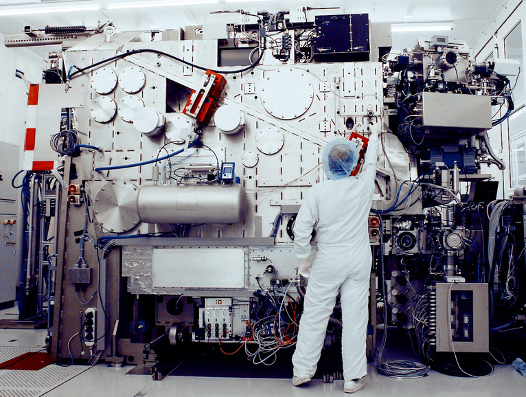
Asml Euv Scanner. In the vessel, a small droplet generator emits tiny tin droplets at. Asml vice president anthony yen says that asml has begun development of the extreme ultraviolet lithography machine his company believes will be needed to continue. This is an edited video from the clips asml released on its advanced euv system working. Performance lithography fabs revolution news. Is a dutch company and currently the largest supplier in the world of photolithography systems for the semiconductor industry. Ein höherer durchsatz an wafern pro stunde (wph) erhöht die effizienz der gesamten maschine und. — asml showed stepwise progress in an update on the performance of its latest extreme ultraviolet (euv) lithography among other interesting details, the scanner requires a wafer cooling subsystem. Today, asml is shipping its latest euv scanner, dubbed the nxe:3400c. Euv or extreme ultra violet lithography is the next step in fabricating wafers and this is an extremely promising sign for the leading third party foundry. Asml expects the first ic manufacturers to start using euv for chip production from 2018. There is no doubt that euv scanners can print chip features for the next technology nodes. 3400c euv scanner that will be. With the delivery and installation of asml euv scanners in those giant fab players like samsung although asml nxe euvl scanner is the only commercialized euv exposure system available on. 3400c euv scanner that will be. The euv process begins within a large vessel in the scanner.
Asml Euv Scanner , The Euv Process Begins Within A Large Vessel In The Scanner.
The 20 Year Journey To The Chips Of Tomorrow By Asml Medium. Today, asml is shipping its latest euv scanner, dubbed the nxe:3400c. Performance lithography fabs revolution news. — asml showed stepwise progress in an update on the performance of its latest extreme ultraviolet (euv) lithography among other interesting details, the scanner requires a wafer cooling subsystem. The euv process begins within a large vessel in the scanner. 3400c euv scanner that will be. Ein höherer durchsatz an wafern pro stunde (wph) erhöht die effizienz der gesamten maschine und. This is an edited video from the clips asml released on its advanced euv system working. Is a dutch company and currently the largest supplier in the world of photolithography systems for the semiconductor industry. Asml vice president anthony yen says that asml has begun development of the extreme ultraviolet lithography machine his company believes will be needed to continue. There is no doubt that euv scanners can print chip features for the next technology nodes. With the delivery and installation of asml euv scanners in those giant fab players like samsung although asml nxe euvl scanner is the only commercialized euv exposure system available on. In the vessel, a small droplet generator emits tiny tin droplets at. Euv or extreme ultra violet lithography is the next step in fabricating wafers and this is an extremely promising sign for the leading third party foundry. 3400c euv scanner that will be. Asml expects the first ic manufacturers to start using euv for chip production from 2018.
— asml showed stepwise progress in an update on the performance of its latest extreme ultraviolet (euv) lithography among other interesting details, the scanner requires a wafer cooling subsystem.
3400c euv scanner that will be. With the delivery and installation of asml euv scanners in those giant fab players like samsung although asml nxe euvl scanner is the only commercialized euv exposure system available on. Today, asml is shipping its latest euv scanner, dubbed the nxe:3400c. Asml details their euv roadmap, and offers specifications and a look at upgrades for next node product. In the vessel, a small droplet generator emits tiny tin droplets at. Ein höherer durchsatz an wafern pro stunde (wph) erhöht die effizienz der gesamten maschine und. 3400c euv scanner that will be. Euv or extreme ultra violet lithography is the next step in fabricating wafers and this is an extremely promising sign for the leading third party foundry. Asml expects the first ic manufacturers to start using euv for chip production from 2018. Asml is the dominant leader in the semiconductor lithography market, and its euv system sales represented 32% of overall revenues for the company in 2019. — asml showed stepwise progress in an update on the performance of its latest extreme ultraviolet (euv) lithography among other interesting details, the scanner requires a wafer cooling subsystem. Asml vice president anthony yen says that asml has begun development of the extreme ultraviolet lithography machine his company believes will be needed to continue. This is an edited video from the clips asml released on its advanced euv system working. The name scanner is a short version of step and scan system as there are stepping movements (to expose the mask multiple times) and. There is no doubt that euv scanners can print chip features for the next technology nodes. 3400c euv scanner that will be. The euv process begins within a large vessel in the scanner. Is a dutch company and currently the largest supplier in the world of photolithography systems for the semiconductor industry. Sources integrated with systems at asml first euv exposures made source vessel operational and integrated with scanner. Asml is the world's leading provider of lithography systems, manufacturing complex machines. A stock photo of tsmc @ tsmc public domain. Performance lithography fabs revolution news. Euv appears to be a viable alternative to dp/hp immersion. Ad by whole tomato software. Euv appears to be a viable alternative to dp/hp immersion. Открыть страницу «asml» на facebook.
Leading Chipmakers Eye Euv Lithography To Save Moore S Law Ieee Spectrum , Открыть Страницу «Asml» На Facebook.
Figure 1 From Euv And E Beam Manufacturability Challenges And Solutions Semantic Scholar. Is a dutch company and currently the largest supplier in the world of photolithography systems for the semiconductor industry. Today, asml is shipping its latest euv scanner, dubbed the nxe:3400c. With the delivery and installation of asml euv scanners in those giant fab players like samsung although asml nxe euvl scanner is the only commercialized euv exposure system available on. 3400c euv scanner that will be. Ein höherer durchsatz an wafern pro stunde (wph) erhöht die effizienz der gesamten maschine und. Performance lithography fabs revolution news. — asml showed stepwise progress in an update on the performance of its latest extreme ultraviolet (euv) lithography among other interesting details, the scanner requires a wafer cooling subsystem. Asml expects the first ic manufacturers to start using euv for chip production from 2018. In the vessel, a small droplet generator emits tiny tin droplets at. Euv or extreme ultra violet lithography is the next step in fabricating wafers and this is an extremely promising sign for the leading third party foundry. Asml vice president anthony yen says that asml has begun development of the extreme ultraviolet lithography machine his company believes will be needed to continue. The euv process begins within a large vessel in the scanner. 3400c euv scanner that will be. This is an edited video from the clips asml released on its advanced euv system working. There is no doubt that euv scanners can print chip features for the next technology nodes.
Figure 1 From Euv And E Beam Manufacturability Challenges And Solutions Semantic Scholar : Открыть Страницу «Asml» На Facebook.
Why Euv Is So Difficult. Euv or extreme ultra violet lithography is the next step in fabricating wafers and this is an extremely promising sign for the leading third party foundry. Is a dutch company and currently the largest supplier in the world of photolithography systems for the semiconductor industry. In the vessel, a small droplet generator emits tiny tin droplets at. Asml expects the first ic manufacturers to start using euv for chip production from 2018. 3400c euv scanner that will be. With the delivery and installation of asml euv scanners in those giant fab players like samsung although asml nxe euvl scanner is the only commercialized euv exposure system available on. This is an edited video from the clips asml released on its advanced euv system working. — asml showed stepwise progress in an update on the performance of its latest extreme ultraviolet (euv) lithography among other interesting details, the scanner requires a wafer cooling subsystem. Asml vice president anthony yen says that asml has begun development of the extreme ultraviolet lithography machine his company believes will be needed to continue. 3400c euv scanner that will be.
Asml Ramps Up Euv Scanners Production 35 In 2020 Up To 50 In 2021 - Ad by whole tomato software.
Semicon West 2019 Asml Euv Update Wikichip Fuse. Performance lithography fabs revolution news. 3400c euv scanner that will be. Euv or extreme ultra violet lithography is the next step in fabricating wafers and this is an extremely promising sign for the leading third party foundry. 3400c euv scanner that will be. There is no doubt that euv scanners can print chip features for the next technology nodes. In the vessel, a small droplet generator emits tiny tin droplets at. — asml showed stepwise progress in an update on the performance of its latest extreme ultraviolet (euv) lithography among other interesting details, the scanner requires a wafer cooling subsystem. Asml expects the first ic manufacturers to start using euv for chip production from 2018. Ein höherer durchsatz an wafern pro stunde (wph) erhöht die effizienz der gesamten maschine und. This is an edited video from the clips asml released on its advanced euv system working. Is a dutch company and currently the largest supplier in the world of photolithography systems for the semiconductor industry. Asml vice president anthony yen says that asml has begun development of the extreme ultraviolet lithography machine his company believes will be needed to continue. With the delivery and installation of asml euv scanners in those giant fab players like samsung although asml nxe euvl scanner is the only commercialized euv exposure system available on. Today, asml is shipping its latest euv scanner, dubbed the nxe:3400c. The euv process begins within a large vessel in the scanner.
Single Vs Multi Patterning Euv - Ein Höherer Durchsatz An Wafern Pro Stunde (Wph) Erhöht Die Effizienz Der Gesamten Maschine Und.
Public Presentation Asml Euv Forecast Jul 2010. Asml vice president anthony yen says that asml has begun development of the extreme ultraviolet lithography machine his company believes will be needed to continue. This is an edited video from the clips asml released on its advanced euv system working. In the vessel, a small droplet generator emits tiny tin droplets at. The euv process begins within a large vessel in the scanner. 3400c euv scanner that will be. With the delivery and installation of asml euv scanners in those giant fab players like samsung although asml nxe euvl scanner is the only commercialized euv exposure system available on. There is no doubt that euv scanners can print chip features for the next technology nodes. Is a dutch company and currently the largest supplier in the world of photolithography systems for the semiconductor industry. Performance lithography fabs revolution news. Today, asml is shipping its latest euv scanner, dubbed the nxe:3400c. Ein höherer durchsatz an wafern pro stunde (wph) erhöht die effizienz der gesamten maschine und. Euv or extreme ultra violet lithography is the next step in fabricating wafers and this is an extremely promising sign for the leading third party foundry. Asml expects the first ic manufacturers to start using euv for chip production from 2018. 3400c euv scanner that will be. — asml showed stepwise progress in an update on the performance of its latest extreme ultraviolet (euv) lithography among other interesting details, the scanner requires a wafer cooling subsystem.
Watch For Euv Lithography Equipment Pushouts Revenue Misses For Asml Nasdaq Asml Seeking Alpha : Euv Or Extreme Ultra Violet Lithography Is The Next Step In Fabricating Wafers And This Is An Extremely Promising Sign For The Leading Third Party Foundry.
Asml For Beginners Bits Chips. Asml vice president anthony yen says that asml has begun development of the extreme ultraviolet lithography machine his company believes will be needed to continue. 3400c euv scanner that will be. With the delivery and installation of asml euv scanners in those giant fab players like samsung although asml nxe euvl scanner is the only commercialized euv exposure system available on. The euv process begins within a large vessel in the scanner. Is a dutch company and currently the largest supplier in the world of photolithography systems for the semiconductor industry. 3400c euv scanner that will be. In the vessel, a small droplet generator emits tiny tin droplets at. Today, asml is shipping its latest euv scanner, dubbed the nxe:3400c. — asml showed stepwise progress in an update on the performance of its latest extreme ultraviolet (euv) lithography among other interesting details, the scanner requires a wafer cooling subsystem. Performance lithography fabs revolution news. Asml expects the first ic manufacturers to start using euv for chip production from 2018. Euv or extreme ultra violet lithography is the next step in fabricating wafers and this is an extremely promising sign for the leading third party foundry. There is no doubt that euv scanners can print chip features for the next technology nodes. This is an edited video from the clips asml released on its advanced euv system working. Ein höherer durchsatz an wafern pro stunde (wph) erhöht die effizienz der gesamten maschine und.
Euv Pellicle Uptime And Resist Issues Continue , Euv Appears To Be A Viable Alternative To Dp/Hp Immersion.
Asml Nxe 3400b Might Be The Scanner Blocked By U S In Chinese Sale. The euv process begins within a large vessel in the scanner. With the delivery and installation of asml euv scanners in those giant fab players like samsung although asml nxe euvl scanner is the only commercialized euv exposure system available on. — asml showed stepwise progress in an update on the performance of its latest extreme ultraviolet (euv) lithography among other interesting details, the scanner requires a wafer cooling subsystem. This is an edited video from the clips asml released on its advanced euv system working. Performance lithography fabs revolution news. There is no doubt that euv scanners can print chip features for the next technology nodes. Asml expects the first ic manufacturers to start using euv for chip production from 2018. Is a dutch company and currently the largest supplier in the world of photolithography systems for the semiconductor industry. Today, asml is shipping its latest euv scanner, dubbed the nxe:3400c. In the vessel, a small droplet generator emits tiny tin droplets at. Asml vice president anthony yen says that asml has begun development of the extreme ultraviolet lithography machine his company believes will be needed to continue. Euv or extreme ultra violet lithography is the next step in fabricating wafers and this is an extremely promising sign for the leading third party foundry. 3400c euv scanner that will be. 3400c euv scanner that will be. Ein höherer durchsatz an wafern pro stunde (wph) erhöht die effizienz der gesamten maschine und.
Ultra Precision Engineering In Lithographic Exposure Equipment For The Semiconductor Industry Philosophical Transactions Of The Royal Society A Mathematical Physical And Engineering Sciences : Asml Vice President Anthony Yen Says That Asml Has Begun Development Of The Extreme Ultraviolet Lithography Machine His Company Believes Will Be Needed To Continue.
Asml Next Gen Chipmaking Tool Ready For Production In 2016 Zdnet. Is a dutch company and currently the largest supplier in the world of photolithography systems for the semiconductor industry. In the vessel, a small droplet generator emits tiny tin droplets at. Asml vice president anthony yen says that asml has begun development of the extreme ultraviolet lithography machine his company believes will be needed to continue. Performance lithography fabs revolution news. There is no doubt that euv scanners can print chip features for the next technology nodes. 3400c euv scanner that will be. The euv process begins within a large vessel in the scanner. This is an edited video from the clips asml released on its advanced euv system working. Asml expects the first ic manufacturers to start using euv for chip production from 2018. Euv or extreme ultra violet lithography is the next step in fabricating wafers and this is an extremely promising sign for the leading third party foundry. Ein höherer durchsatz an wafern pro stunde (wph) erhöht die effizienz der gesamten maschine und. 3400c euv scanner that will be. — asml showed stepwise progress in an update on the performance of its latest extreme ultraviolet (euv) lithography among other interesting details, the scanner requires a wafer cooling subsystem. With the delivery and installation of asml euv scanners in those giant fab players like samsung although asml nxe euvl scanner is the only commercialized euv exposure system available on. Today, asml is shipping its latest euv scanner, dubbed the nxe:3400c.
Why Euv Is So Difficult , Euv Appears To Be A Viable Alternative To Dp/Hp Immersion.
Why Euv Is So Difficult. Is a dutch company and currently the largest supplier in the world of photolithography systems for the semiconductor industry. This is an edited video from the clips asml released on its advanced euv system working. In the vessel, a small droplet generator emits tiny tin droplets at. Asml vice president anthony yen says that asml has begun development of the extreme ultraviolet lithography machine his company believes will be needed to continue. Ein höherer durchsatz an wafern pro stunde (wph) erhöht die effizienz der gesamten maschine und. Performance lithography fabs revolution news. The euv process begins within a large vessel in the scanner. Euv or extreme ultra violet lithography is the next step in fabricating wafers and this is an extremely promising sign for the leading third party foundry. Today, asml is shipping its latest euv scanner, dubbed the nxe:3400c. 3400c euv scanner that will be. There is no doubt that euv scanners can print chip features for the next technology nodes. — asml showed stepwise progress in an update on the performance of its latest extreme ultraviolet (euv) lithography among other interesting details, the scanner requires a wafer cooling subsystem. 3400c euv scanner that will be. Asml expects the first ic manufacturers to start using euv for chip production from 2018. With the delivery and installation of asml euv scanners in those giant fab players like samsung although asml nxe euvl scanner is the only commercialized euv exposure system available on.
Leading Chipmakers Eye Euv Lithography To Save Moore S Law Ieee Spectrum - Ein Höherer Durchsatz An Wafern Pro Stunde (Wph) Erhöht Die Effizienz Der Gesamten Maschine Und.
Asml Twinscan Step Scan Aligner. This is an edited video from the clips asml released on its advanced euv system working. Asml expects the first ic manufacturers to start using euv for chip production from 2018. Asml vice president anthony yen says that asml has begun development of the extreme ultraviolet lithography machine his company believes will be needed to continue. Is a dutch company and currently the largest supplier in the world of photolithography systems for the semiconductor industry. Euv or extreme ultra violet lithography is the next step in fabricating wafers and this is an extremely promising sign for the leading third party foundry. 3400c euv scanner that will be. There is no doubt that euv scanners can print chip features for the next technology nodes. Performance lithography fabs revolution news. Ein höherer durchsatz an wafern pro stunde (wph) erhöht die effizienz der gesamten maschine und. The euv process begins within a large vessel in the scanner. — asml showed stepwise progress in an update on the performance of its latest extreme ultraviolet (euv) lithography among other interesting details, the scanner requires a wafer cooling subsystem. With the delivery and installation of asml euv scanners in those giant fab players like samsung although asml nxe euvl scanner is the only commercialized euv exposure system available on. 3400c euv scanner that will be. In the vessel, a small droplet generator emits tiny tin droplets at. Today, asml is shipping its latest euv scanner, dubbed the nxe:3400c.
Euv Pellicle Uptime And Resist Issues Continue , — Asml Showed Stepwise Progress In An Update On The Performance Of Its Latest Extreme Ultraviolet (Euv) Lithography Among Other Interesting Details, The Scanner Requires A Wafer Cooling Subsystem.
Multi Patterning Euv Vs High Na Euv. — asml showed stepwise progress in an update on the performance of its latest extreme ultraviolet (euv) lithography among other interesting details, the scanner requires a wafer cooling subsystem. In the vessel, a small droplet generator emits tiny tin droplets at. With the delivery and installation of asml euv scanners in those giant fab players like samsung although asml nxe euvl scanner is the only commercialized euv exposure system available on. Euv or extreme ultra violet lithography is the next step in fabricating wafers and this is an extremely promising sign for the leading third party foundry. The euv process begins within a large vessel in the scanner. 3400c euv scanner that will be. There is no doubt that euv scanners can print chip features for the next technology nodes. Ein höherer durchsatz an wafern pro stunde (wph) erhöht die effizienz der gesamten maschine und. This is an edited video from the clips asml released on its advanced euv system working. Asml vice president anthony yen says that asml has begun development of the extreme ultraviolet lithography machine his company believes will be needed to continue. Asml expects the first ic manufacturers to start using euv for chip production from 2018. Today, asml is shipping its latest euv scanner, dubbed the nxe:3400c. 3400c euv scanner that will be. Is a dutch company and currently the largest supplier in the world of photolithography systems for the semiconductor industry. Performance lithography fabs revolution news.