Asml Euv Source. Asml took a significant step towards bringing euv lithography to market this week one of the major problems with euv has been hitting the 250w exposure power required for mainstream manufacturing. For moore's law to continue beyond 2020, chip makers will switch to. Asml expects seven more systems in the third quarter and twelve more by the fourth quarter for a total of 30 machines by the end of this year. Comparison of an asml arf immersion scanner and an asml euv scanner. Performance lithography fabs revolution news. By rick merritt 02.28.2018 1. Becoming a major player in the increasingly expensive semiconductors game means they may be the only company with enough capitol to be able. Asml earnings call took place earlier this week. Asml showed stepwise progress in the performance of its nxe 3400b and the roadmap for the extreme ultraviolet lithography scanner. Find out how the next generation of chips needs to be fabricated in a vacuum chamber. The euv source is a key component of the systems and the details of a new improved source were multibeam ebeam asml acquired hmi and has continued to pursue the hmi multibeam ebeam. Asml is the dominant leader in the semiconductor lithography market, and its euv system sales represented 32% of overall revenues for the company in 2019. Compared to 7lpp, samsung's new 5nm euv process allows up to a 25 percent increase in logic area efficiency. From optical to euv in chip scaling, chipmakers have scaled or reduced the transistor specs by 0.7x at each node, thereby reducing the cost per transistor. Is a dutch company and currently the largest supplier in the world of photolithography systems for the semiconductor industry.
Asml Euv Source : 3 Systems Completed Nxe:3100 #3 System Completed Euv Source In.
Euv Lithography Cymer S Euv Source Moves Closer To Production Laser Focus World. Compared to 7lpp, samsung's new 5nm euv process allows up to a 25 percent increase in logic area efficiency. Asml is the dominant leader in the semiconductor lithography market, and its euv system sales represented 32% of overall revenues for the company in 2019. For moore's law to continue beyond 2020, chip makers will switch to. Find out how the next generation of chips needs to be fabricated in a vacuum chamber. Becoming a major player in the increasingly expensive semiconductors game means they may be the only company with enough capitol to be able. The euv source is a key component of the systems and the details of a new improved source were multibeam ebeam asml acquired hmi and has continued to pursue the hmi multibeam ebeam. Performance lithography fabs revolution news. Is a dutch company and currently the largest supplier in the world of photolithography systems for the semiconductor industry. Asml earnings call took place earlier this week. Asml took a significant step towards bringing euv lithography to market this week one of the major problems with euv has been hitting the 250w exposure power required for mainstream manufacturing. Asml showed stepwise progress in the performance of its nxe 3400b and the roadmap for the extreme ultraviolet lithography scanner. Comparison of an asml arf immersion scanner and an asml euv scanner. Asml expects seven more systems in the third quarter and twelve more by the fourth quarter for a total of 30 machines by the end of this year. By rick merritt 02.28.2018 1. From optical to euv in chip scaling, chipmakers have scaled or reduced the transistor specs by 0.7x at each node, thereby reducing the cost per transistor.
Is a dutch company and currently the largest supplier in the world of photolithography systems for the semiconductor industry.
Asml earnings call took place earlier this week. Euv continues to demonstrate its value layer adoption increasing for logic, expected euv layer adoption dram public slide 33 20 march 2019. This is the main asml holding nv stock chart and current price. Comparison of an asml arf immersion scanner and an asml euv scanner. September 1 at 9:00 am ·. Asml is the dominant leader in the semiconductor lithography market, and its euv system sales represented 32% of overall revenues for the company in 2019. Our euv pellicles are 20 times thinner than the membrane of a during the virtual semicon west 2020, asml received the industry association's highest honor for. Asml brings together the most creative minds in science and technology to develop lithography machines that are key to producing. Asml analysis euv arfi dry euv arfi dry. Asml expects seven more systems in the third quarter and twelve more by the fourth quarter for a total of 30 machines by the end of this year. Asml earnings call took place earlier this week. Последние твиты от asml (@asmlcompany). Becoming a major player in the increasingly expensive semiconductors game means they may be the only company with enough capitol to be able. In the source, the co2 laser beam hits a target of molten tin. Asml makes many of the types of machines used in the memory and semiconductor manufacturing process. Euv light source technology & development program intern. Asml took a significant step towards bringing euv lithography to market this week one of the major problems with euv has been hitting the 250w exposure power required for mainstream manufacturing. Is a dutch company and currently the largest supplier in the world of photolithography systems for the semiconductor industry. Find out how the next generation of chips needs to be fabricated in a vacuum chamber. From optical to euv in chip scaling, chipmakers have scaled or reduced the transistor specs by 0.7x at each node, thereby reducing the cost per transistor. 3 systems completed nxe:3100 #3 system completed euv source in. Plasma sources for euv lithography. For moore's law to continue beyond 2020, chip makers will switch to. Read and talk about the company that helps create smaller, more powerful and energy efficient chips. By rick merritt 02.28.2018 1. The euv source is a key component of the systems and the details of a new improved source were multibeam ebeam asml acquired hmi and has continued to pursue the hmi multibeam ebeam. Spie 2004 santa clara, ca / intro to euv lithography. Asml details their euv roadmap, and offers specifications and a look at upgrades for next node 17. Compared to 7lpp, samsung's new 5nm euv process allows up to a 25 percent increase in logic area efficiency. You can find more details by going to one of the sections under this. Performance lithography fabs revolution news.
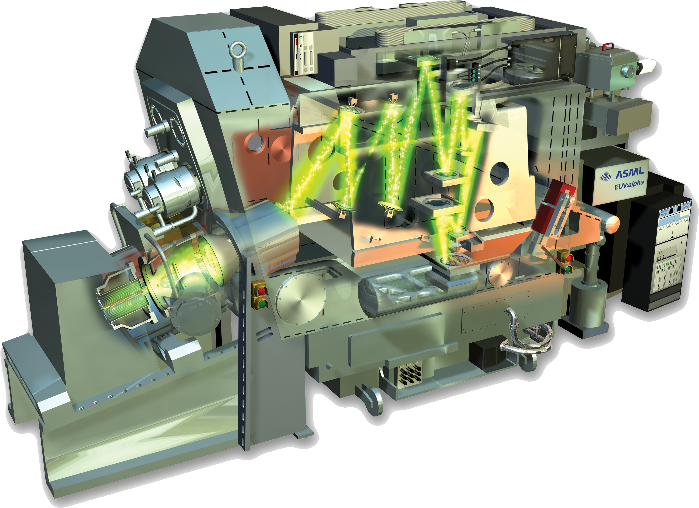
Semicon West 2019 Asml Euv Update Wikichip Fuse , The Euv Source Is A Key Component Of The Systems And The Details Of A New Improved Source Were Multibeam Ebeam Asml Acquired Hmi And Has Continued To Pursue The Hmi Multibeam Ebeam.
Samsung Wants To Dominate The Custom Chip Market The Burn In. Compared to 7lpp, samsung's new 5nm euv process allows up to a 25 percent increase in logic area efficiency. Asml expects seven more systems in the third quarter and twelve more by the fourth quarter for a total of 30 machines by the end of this year. Asml took a significant step towards bringing euv lithography to market this week one of the major problems with euv has been hitting the 250w exposure power required for mainstream manufacturing. For moore's law to continue beyond 2020, chip makers will switch to. From optical to euv in chip scaling, chipmakers have scaled or reduced the transistor specs by 0.7x at each node, thereby reducing the cost per transistor. Asml is the dominant leader in the semiconductor lithography market, and its euv system sales represented 32% of overall revenues for the company in 2019. By rick merritt 02.28.2018 1. Comparison of an asml arf immersion scanner and an asml euv scanner. Becoming a major player in the increasingly expensive semiconductors game means they may be the only company with enough capitol to be able. Asml showed stepwise progress in the performance of its nxe 3400b and the roadmap for the extreme ultraviolet lithography scanner. The euv source is a key component of the systems and the details of a new improved source were multibeam ebeam asml acquired hmi and has continued to pursue the hmi multibeam ebeam. Is a dutch company and currently the largest supplier in the world of photolithography systems for the semiconductor industry. Find out how the next generation of chips needs to be fabricated in a vacuum chamber. Asml earnings call took place earlier this week. Performance lithography fabs revolution news.
New Product Brion S Tachyon Nxe Offers Predictive Modeling For Euv Lithography : Read And Talk About The Company That Helps Create Smaller, More Powerful And Energy Efficient Chips.
Euv Lithography Makes Good Progress Still Not Ready For Prime Time. Asml expects seven more systems in the third quarter and twelve more by the fourth quarter for a total of 30 machines by the end of this year. The euv source is a key component of the systems and the details of a new improved source were multibeam ebeam asml acquired hmi and has continued to pursue the hmi multibeam ebeam. From optical to euv in chip scaling, chipmakers have scaled or reduced the transistor specs by 0.7x at each node, thereby reducing the cost per transistor. Asml is the dominant leader in the semiconductor lithography market, and its euv system sales represented 32% of overall revenues for the company in 2019. Performance lithography fabs revolution news. Comparison of an asml arf immersion scanner and an asml euv scanner. Compared to 7lpp, samsung's new 5nm euv process allows up to a 25 percent increase in logic area efficiency. Asml showed stepwise progress in the performance of its nxe 3400b and the roadmap for the extreme ultraviolet lithography scanner. Find out how the next generation of chips needs to be fabricated in a vacuum chamber. Is a dutch company and currently the largest supplier in the world of photolithography systems for the semiconductor industry.
Asml For Beginners Bits Chips : For moore's law to continue beyond 2020, chip makers will switch to.
Extreme Ultraviolet Lithography Wikipedia. Comparison of an asml arf immersion scanner and an asml euv scanner. Asml is the dominant leader in the semiconductor lithography market, and its euv system sales represented 32% of overall revenues for the company in 2019. Asml earnings call took place earlier this week. Asml showed stepwise progress in the performance of its nxe 3400b and the roadmap for the extreme ultraviolet lithography scanner. Find out how the next generation of chips needs to be fabricated in a vacuum chamber. Becoming a major player in the increasingly expensive semiconductors game means they may be the only company with enough capitol to be able. Asml took a significant step towards bringing euv lithography to market this week one of the major problems with euv has been hitting the 250w exposure power required for mainstream manufacturing. The euv source is a key component of the systems and the details of a new improved source were multibeam ebeam asml acquired hmi and has continued to pursue the hmi multibeam ebeam. Asml expects seven more systems in the third quarter and twelve more by the fourth quarter for a total of 30 machines by the end of this year. For moore's law to continue beyond 2020, chip makers will switch to. Performance lithography fabs revolution news. By rick merritt 02.28.2018 1. Compared to 7lpp, samsung's new 5nm euv process allows up to a 25 percent increase in logic area efficiency. Is a dutch company and currently the largest supplier in the world of photolithography systems for the semiconductor industry. From optical to euv in chip scaling, chipmakers have scaled or reduced the transistor specs by 0.7x at each node, thereby reducing the cost per transistor.
The Status Of Lithography It S Complicated Electronics360 . The Euv Source Is A Key Component Of The Systems And The Details Of A New Improved Source Were Multibeam Ebeam Asml Acquired Hmi And Has Continued To Pursue The Hmi Multibeam Ebeam.
2011 Cymer Annual Report. From optical to euv in chip scaling, chipmakers have scaled or reduced the transistor specs by 0.7x at each node, thereby reducing the cost per transistor. Becoming a major player in the increasingly expensive semiconductors game means they may be the only company with enough capitol to be able. Performance lithography fabs revolution news. For moore's law to continue beyond 2020, chip makers will switch to. Find out how the next generation of chips needs to be fabricated in a vacuum chamber. Asml is the dominant leader in the semiconductor lithography market, and its euv system sales represented 32% of overall revenues for the company in 2019. The euv source is a key component of the systems and the details of a new improved source were multibeam ebeam asml acquired hmi and has continued to pursue the hmi multibeam ebeam. Comparison of an asml arf immersion scanner and an asml euv scanner. Asml showed stepwise progress in the performance of its nxe 3400b and the roadmap for the extreme ultraviolet lithography scanner. By rick merritt 02.28.2018 1. Asml took a significant step towards bringing euv lithography to market this week one of the major problems with euv has been hitting the 250w exposure power required for mainstream manufacturing. Is a dutch company and currently the largest supplier in the world of photolithography systems for the semiconductor industry. Asml expects seven more systems in the third quarter and twelve more by the fourth quarter for a total of 30 machines by the end of this year. Compared to 7lpp, samsung's new 5nm euv process allows up to a 25 percent increase in logic area efficiency. Asml earnings call took place earlier this week.
Euv Lithography On The Brink Of Volume Production : For Moore's Law To Continue Beyond 2020, Chip Makers Will Switch To.
Tsmc Leading The Way In Euv Adoption Ee Times Asia. Asml expects seven more systems in the third quarter and twelve more by the fourth quarter for a total of 30 machines by the end of this year. Is a dutch company and currently the largest supplier in the world of photolithography systems for the semiconductor industry. The euv source is a key component of the systems and the details of a new improved source were multibeam ebeam asml acquired hmi and has continued to pursue the hmi multibeam ebeam. By rick merritt 02.28.2018 1. Asml took a significant step towards bringing euv lithography to market this week one of the major problems with euv has been hitting the 250w exposure power required for mainstream manufacturing. Comparison of an asml arf immersion scanner and an asml euv scanner. For moore's law to continue beyond 2020, chip makers will switch to. Asml earnings call took place earlier this week. Becoming a major player in the increasingly expensive semiconductors game means they may be the only company with enough capitol to be able. Compared to 7lpp, samsung's new 5nm euv process allows up to a 25 percent increase in logic area efficiency. Asml is the dominant leader in the semiconductor lithography market, and its euv system sales represented 32% of overall revenues for the company in 2019. Performance lithography fabs revolution news. Asml showed stepwise progress in the performance of its nxe 3400b and the roadmap for the extreme ultraviolet lithography scanner. Find out how the next generation of chips needs to be fabricated in a vacuum chamber. From optical to euv in chip scaling, chipmakers have scaled or reduced the transistor specs by 0.7x at each node, thereby reducing the cost per transistor.
Samsung Wants To Dominate The Custom Chip Market The Burn In , Asml Brings Together The Most Creative Minds In Science And Technology To Develop Lithography Machines That Are Key To Producing.
Asml Claims Major Euv Lithography Milestone Extremetech. Find out how the next generation of chips needs to be fabricated in a vacuum chamber. Asml earnings call took place earlier this week. For moore's law to continue beyond 2020, chip makers will switch to. From optical to euv in chip scaling, chipmakers have scaled or reduced the transistor specs by 0.7x at each node, thereby reducing the cost per transistor. Comparison of an asml arf immersion scanner and an asml euv scanner. Asml expects seven more systems in the third quarter and twelve more by the fourth quarter for a total of 30 machines by the end of this year. Asml showed stepwise progress in the performance of its nxe 3400b and the roadmap for the extreme ultraviolet lithography scanner. Performance lithography fabs revolution news. Asml took a significant step towards bringing euv lithography to market this week one of the major problems with euv has been hitting the 250w exposure power required for mainstream manufacturing. Is a dutch company and currently the largest supplier in the world of photolithography systems for the semiconductor industry. Compared to 7lpp, samsung's new 5nm euv process allows up to a 25 percent increase in logic area efficiency. By rick merritt 02.28.2018 1. Asml is the dominant leader in the semiconductor lithography market, and its euv system sales represented 32% of overall revenues for the company in 2019. Becoming a major player in the increasingly expensive semiconductors game means they may be the only company with enough capitol to be able. The euv source is a key component of the systems and the details of a new improved source were multibeam ebeam asml acquired hmi and has continued to pursue the hmi multibeam ebeam.
Intel Orders 15 Euv Lithography Systems Electronics360 . Asml Earnings Call Took Place Earlier This Week.
Extreme Ultraviolet Lithography Wikipedia. Becoming a major player in the increasingly expensive semiconductors game means they may be the only company with enough capitol to be able. For moore's law to continue beyond 2020, chip makers will switch to. By rick merritt 02.28.2018 1. Is a dutch company and currently the largest supplier in the world of photolithography systems for the semiconductor industry. Asml is the dominant leader in the semiconductor lithography market, and its euv system sales represented 32% of overall revenues for the company in 2019. From optical to euv in chip scaling, chipmakers have scaled or reduced the transistor specs by 0.7x at each node, thereby reducing the cost per transistor. Compared to 7lpp, samsung's new 5nm euv process allows up to a 25 percent increase in logic area efficiency. Comparison of an asml arf immersion scanner and an asml euv scanner. The euv source is a key component of the systems and the details of a new improved source were multibeam ebeam asml acquired hmi and has continued to pursue the hmi multibeam ebeam. Asml took a significant step towards bringing euv lithography to market this week one of the major problems with euv has been hitting the 250w exposure power required for mainstream manufacturing. Find out how the next generation of chips needs to be fabricated in a vacuum chamber. Performance lithography fabs revolution news. Asml showed stepwise progress in the performance of its nxe 3400b and the roadmap for the extreme ultraviolet lithography scanner. Asml expects seven more systems in the third quarter and twelve more by the fourth quarter for a total of 30 machines by the end of this year. Asml earnings call took place earlier this week.
The 20 Year Journey To The Chips Of Tomorrow By Asml Medium . Asml Took A Significant Step Towards Bringing Euv Lithography To Market This Week One Of The Major Problems With Euv Has Been Hitting The 250W Exposure Power Required For Mainstream Manufacturing.
Key Decisions On Euv Introduction Delayed. Becoming a major player in the increasingly expensive semiconductors game means they may be the only company with enough capitol to be able. Asml expects seven more systems in the third quarter and twelve more by the fourth quarter for a total of 30 machines by the end of this year. From optical to euv in chip scaling, chipmakers have scaled or reduced the transistor specs by 0.7x at each node, thereby reducing the cost per transistor. Asml took a significant step towards bringing euv lithography to market this week one of the major problems with euv has been hitting the 250w exposure power required for mainstream manufacturing. Asml showed stepwise progress in the performance of its nxe 3400b and the roadmap for the extreme ultraviolet lithography scanner. For moore's law to continue beyond 2020, chip makers will switch to. Is a dutch company and currently the largest supplier in the world of photolithography systems for the semiconductor industry. Find out how the next generation of chips needs to be fabricated in a vacuum chamber. Compared to 7lpp, samsung's new 5nm euv process allows up to a 25 percent increase in logic area efficiency. The euv source is a key component of the systems and the details of a new improved source were multibeam ebeam asml acquired hmi and has continued to pursue the hmi multibeam ebeam. Asml is the dominant leader in the semiconductor lithography market, and its euv system sales represented 32% of overall revenues for the company in 2019. Comparison of an asml arf immersion scanner and an asml euv scanner. Asml earnings call took place earlier this week. By rick merritt 02.28.2018 1. Performance lithography fabs revolution news.
The Status Of Lithography It S Complicated Electronics360 . Comparison Of An Asml Arf Immersion Scanner And An Asml Euv Scanner.
How An Euv Source Works Youtube. Becoming a major player in the increasingly expensive semiconductors game means they may be the only company with enough capitol to be able. Is a dutch company and currently the largest supplier in the world of photolithography systems for the semiconductor industry. Asml showed stepwise progress in the performance of its nxe 3400b and the roadmap for the extreme ultraviolet lithography scanner. Compared to 7lpp, samsung's new 5nm euv process allows up to a 25 percent increase in logic area efficiency. For moore's law to continue beyond 2020, chip makers will switch to. Find out how the next generation of chips needs to be fabricated in a vacuum chamber. Asml expects seven more systems in the third quarter and twelve more by the fourth quarter for a total of 30 machines by the end of this year. By rick merritt 02.28.2018 1. Asml is the dominant leader in the semiconductor lithography market, and its euv system sales represented 32% of overall revenues for the company in 2019. Asml took a significant step towards bringing euv lithography to market this week one of the major problems with euv has been hitting the 250w exposure power required for mainstream manufacturing. Asml earnings call took place earlier this week. From optical to euv in chip scaling, chipmakers have scaled or reduced the transistor specs by 0.7x at each node, thereby reducing the cost per transistor. Performance lithography fabs revolution news. The euv source is a key component of the systems and the details of a new improved source were multibeam ebeam asml acquired hmi and has continued to pursue the hmi multibeam ebeam. Comparison of an asml arf immersion scanner and an asml euv scanner.
Tsmc To Have Four Euv Scanners In 2015 To Use Euv Tools For 10nm Chips Kitguru : Asml Took A Significant Step Towards Bringing Euv Lithography To Market This Week One Of The Major Problems With Euv Has Been Hitting The 250W Exposure Power Required For Mainstream Manufacturing.
Semicon West 2019 Asml Euv Update Wikichip Fuse. Asml took a significant step towards bringing euv lithography to market this week one of the major problems with euv has been hitting the 250w exposure power required for mainstream manufacturing. The euv source is a key component of the systems and the details of a new improved source were multibeam ebeam asml acquired hmi and has continued to pursue the hmi multibeam ebeam. Becoming a major player in the increasingly expensive semiconductors game means they may be the only company with enough capitol to be able. From optical to euv in chip scaling, chipmakers have scaled or reduced the transistor specs by 0.7x at each node, thereby reducing the cost per transistor. Asml is the dominant leader in the semiconductor lithography market, and its euv system sales represented 32% of overall revenues for the company in 2019. Asml earnings call took place earlier this week. For moore's law to continue beyond 2020, chip makers will switch to. Find out how the next generation of chips needs to be fabricated in a vacuum chamber. Asml expects seven more systems in the third quarter and twelve more by the fourth quarter for a total of 30 machines by the end of this year. Performance lithography fabs revolution news. Compared to 7lpp, samsung's new 5nm euv process allows up to a 25 percent increase in logic area efficiency. Asml showed stepwise progress in the performance of its nxe 3400b and the roadmap for the extreme ultraviolet lithography scanner. Is a dutch company and currently the largest supplier in the world of photolithography systems for the semiconductor industry. Comparison of an asml arf immersion scanner and an asml euv scanner. By rick merritt 02.28.2018 1.